From a hardware perspective, the only thing needed to load and run a program on JStamp are power and some way to connect the JTAG cable to JStamp. That can theoretically be rigged up using a solderless breadboard, but the JTAG cable must be powered with 5 volts (regulated) from the JStamp end. That makes the solderless breadboard approach rather complicated.
Fortunately, the JStamp Development Station makes this very easy. It also includes a number of additional components that greatly simplify the interface between JStamp and the external world beyond the development system. Details of the JStamp Development Station can be found on the JStamp web site. Note that once a JStamp has been programmed, it can be easily deployed into your own custom circuit, including on a solderless breadboard.
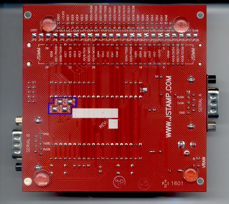
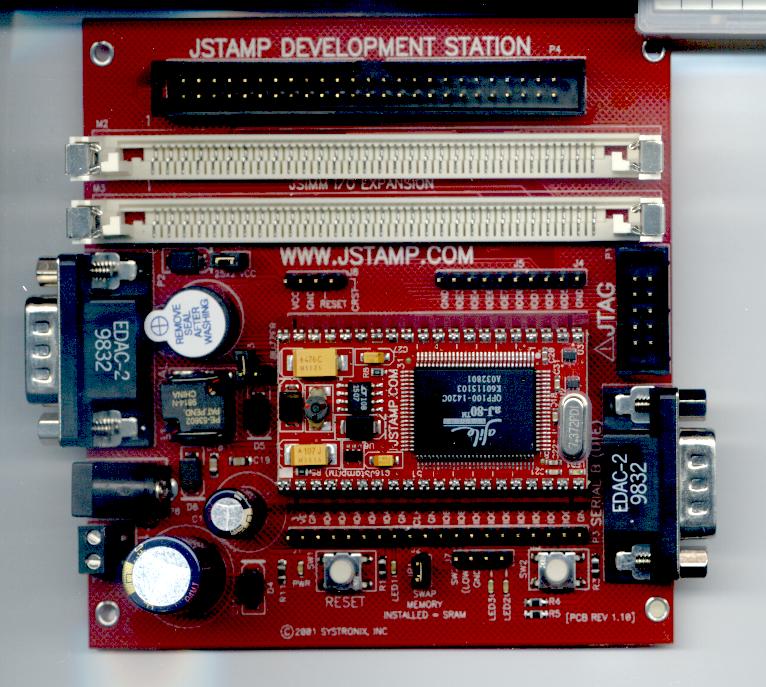
Close-up images of the top and bottom of the JStamp Development Station are shown here.
The top view shows the JStamp Development Station with the JStamp in place. You'll also note in the lower left corner that this is PCB rev 1.10. The only(?) significant difference between PCB rev 1.10 and PCB rev 1 is outlined in blue on the bottom view. This image was scanned at 160 DPI with the JStamp Development Station resting directly on the scanner glass.
This is the bottom view of the JStamp Development Station. The four solder paste jumpers outlined in blue were added to PCB rev 1.10 to allow for easy isolation of the RS-232 level shifters. This image was scanned at 160 DPI with the JStamp Development Station resting directly on the scanner glass.