This page contains detailed close-up images of JStamp and smaller images that highlight JStamp significant parts.
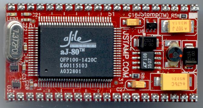
Detailed close-up image of the top side of
JStamp
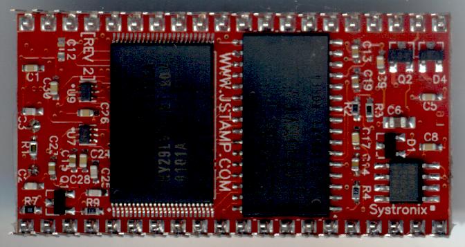
Detailed close-up image of the bottom side
of JStamp
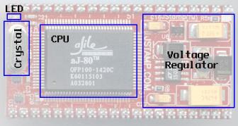
Significant parts on the top side of
JStamp
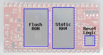
Significant parts on the bottom side of
JStamp
This image shows the top of JStamp in great detail. It was scanned at 320 DPI with the JStamp resting directly on the scanner glass. A smaller image below highlights the significant parts on the top of the JStamp.
This image shows the bottom of JStamp in great detail. It was scanned at 320 DPI with the JStamp resting directly on the scanner glass. A smaller image below highlights the significant parts on the bottom of JStamp.
This image highlights the significant parts on the top side of JStamp. The top side of JStamp contains the aJ-80 processor (CPU), voltage regulator, LED, and crystal.
This image highlights the significant parts on the bottom side of JStamp. The bottom side of JStamp contains the flash ROM, static RAM, and reset circuitry. In addition to debouncing an external reset push button switch, the reset circuitry serves another important, if unglamorous, purpose. It monitors the regulated supply voltages and holds the processor in a reset state whenever the voltages dip below acceptable levels. This is critical to prevent erratic system operation when supply voltages dwindle (such as when a battery runs low).